There is a lot going on in the field of the highest speed network ASICs. These are focused on very high speed, less features, and lower buffers, driven by the hyperscalers and the Financial industry which desires the lowest latency switching. This is a rich area that I can’t cover completely even in this long post. There’s a lot more to dive into, but hopefully this will give you a taste and somethings to chase after if you want more understanding.
An Application Specific Integrated Circuit (ASIC) is purpose built for a particular use. In this case, these are built to provide as much network throughput as possible. They are two orders of magnitude faster than Intel CPUs for forwarding packets. While these ASICs can do x Billion PPS, with careful software work, Intel CPUs can do x 10s of Millions PPS. If you want to cost effectively switch billions of PPS or terabits of traffic you will use an ASIC and not a general purpose CPU.
The use of these high speed ASICs in networking was really started by Broadcom and Fulcrum in the mid 2000s. Fulcrum Terabit Clockless Crossbar switch is a document from 2003, just the beginning for Fulcrum. They were using 130nm technology and building 1M transistor parts. We’ll talk about what those mean later in this post. This chip wasn’t even Ethernet, it’s purpose was to be in the middle of other network (Ethernet) processing chips and just be the switch. Later generations were L2, and then they created an L3 switch. Fulcrum’s first Ethernet ASICs at 24 ports of 10G were the chips Arista used to get started.
These chips (and others with more functionality and/or lower speeds) are sometimes called merchant silicon, meaning that these vendors sell these chips to other parties which might build systems including software around them. All network vendors use these merchant silicon in at least some of their routers and switches. These are also used by all the big cloud companies and anybody talking about disaggregated networks. Some network vendors also create their own ASICs. Arista uses all merchant silicon; Juniper and Cisco use some proprietary and some merchant silicon.
Over half of the Ethernet switches that ship now, ship with Merchant Silicon.
How they work and how they are different from chips in Chassis
For the most part, the ASICs that we are talking about here work as a single ASIC in the device. Meaning that there are other chips such as Ethernet MACs and CPUs, but all the network forwarding decisions and buffering are done inside one chip. Historically these chips have been used for ToR switches, but some networks especially hyperscalers are using them throughout the network, usually in the form of small fixed form factor (pizza boxes.) Some people do combine them in interesting ways such as Facebook’s minipack.
In any chip design there is a fixed budget of resources, which are: transistors, space on the chip die, and the number of pins from the chip to the rest of the system. If you want more of one set of features then you have to give up something else. These chips are optimized for the most speed in terms of Ethernet ports, so they have a lot of their die tied up in getting data off the chip to the interfaces. One of the consequences is that they have much less buffering and table space than other chips. You might say well “Why can’t they use off chip TCAM or buffers?” First, to use off chip resources means that you are using pins and chip real-estate that you wanted to use for providing more interface speed. Second, off chip memory is slower and higher latency so that it would slow down the packet-per-second rate.
There are chipsets that work together to form large chassis devices and there are even merchant silicon than does this. The most popular in merchant silicon of these chips is the Broadcom Strata DNX. For instance, the Arista 7500 is based on this chipset. There are two big advantages to this kind of chipset: they work together to build a larger system to support more ports and because they are not a single chip, they can handle off-chip table and buffer space, so these have 1M+ table space and large buffers. These chips are also used in fixed form-factor devices that have large enough tables for the internet. Any individual one of these chips has less throughput than the chips we’ve been focusing on because they must spend more of their resources accessing and connecting to other chips in the system.
Important architecture considerations
There are many different designs decisions that are chosen and we want to understand the impact of those.
Node size and transistor count
Effectively all of the companies that build these chips are called fabless semiconductor design firms, which means that they design the chips, but they don’t physically create them. A Fab is the Fabrication plant that these chips are made. The largest is TSMC, which I think makes most of these chips, if not all.
The ASICs we are focused on are almost as big as it’s possible to make a chip with. It turns out that there is a limit to the size of chip that can be made in state-of-the-art fabrication plants (fabs), which is called the Reticle limit which is 33x26 mm. I do not understand the physics or any of this process to understand why that is but it means that the absolute max size is 858mm^2. Nvidia’s next gen chip GA100 is 54.2 billion transistors and a die size of 826mm^2 using 7nm processor node.
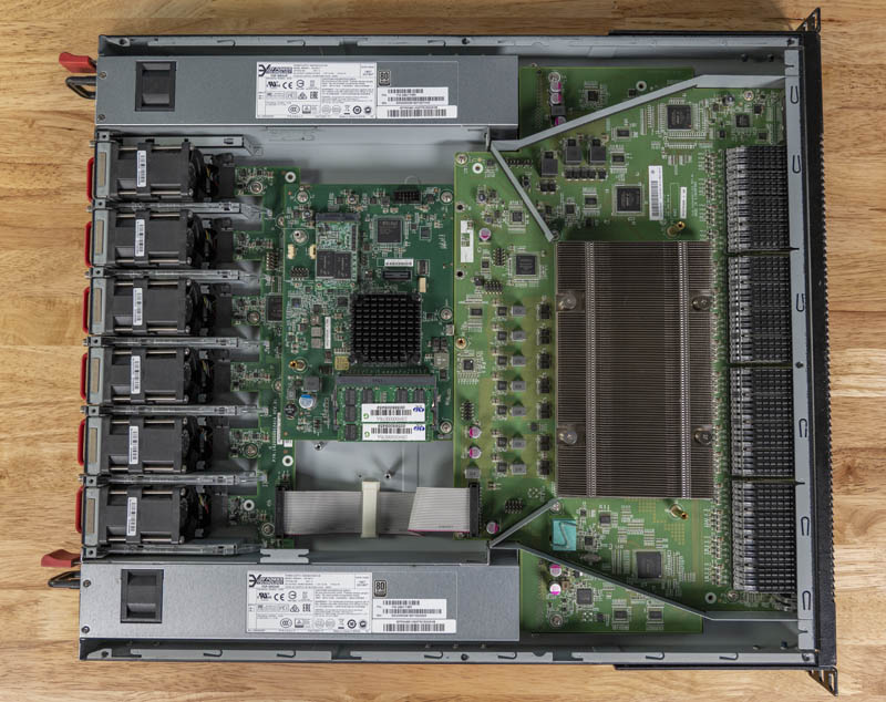 This is a picture of a switch with a heatsink on the Tomahawk 1.
Another important number to understand is the process node size which is a measure of the size of the transistors. Current state-of-the-art is 7nm, though Apple has just released a 5nm CPU. The advantage of smaller node size the more transistors you can get on the chip. In the past several decades Intel has always had the smallest process node size, until the last couple years. Smaller node sizes always go to the biggest money maker and so for TSMC and other fabs like it those are now mobile processors. So 7nm mobile phone CPUs came out first. These are not big chips, but there are billions of them. Soon after comes GPUs which are about as big of chips as you can make. And soon after that are these network ASICs which are as big as the GPU.
One aspect of all this comes out in the amount of power that a chip consumes. Some of these are very power hungry, which makes them hard to power and harder to cool. The design of these chips take a lot of money. It’s very interesting how many different companies are trying to compete at this time and how much money some of them have raised.
It’s also interesting to note when a company moves to a smaller process size and when another company stays at the size they were using before. I don’t know why moving to smaller node size requires design and engineering work, but it does, so to mitigate that design work some companies move earlier than others to new node sizes.
IP and SERDES
When talking about Integrated Circuits (ICs), IP means something different than most of us network engineers think. It means Intellectual Property, which is a reusable unit of logic. For instance, ARM sells IP blocks to all it’s customers to make all of the CPUs that everybody uses in their mobile phones.
You don’t have to buy the IP block for the whole chip. For instance, there’s a really important IP block in these chips called the Serializer/Deserializer (SerDes). This is the part of the chip that gets data in/out of the chip to the pins. Not everyone of these companies makes their own SerDes, many actually get their SerDes from Broadcom or Avago, which is now also Broadcom. It’s interesting to try to keep track of how much influence Broadcom has.
SERDES and related topics deserve their own article of similar size, but that’s for another time (and probably another more qualified person.)
Chiplets
One way to keep up with the complexity and size of these chips is to break them up into what is called a chiplet. These are blocks of IP that are then put together in an end product. Since they are smaller than one chip, you can take advantage of the fact that you will suffer less effects from manufacturing errors. Apple and other ARM customers have been doing chiplets for several years, and AMD is now doing that in their CPUs.
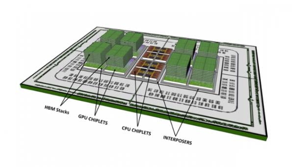
Some of these high throughput network ASICs are using chiplets and some are not. Chiplets are the way of the future for many IC designs. Several of these Network ASICs use chiplets (see the table below), as does Apple in their A* CPUs, while Broadcom Ethernet switches do not.
Pipelines and Buffers
Just like in CPUs, we’ve gotten to a place where you have to have multiple cores to take advantage of the transistors available in these ASICs. They have multiple pipelines that are interacting together to get the performance required. This is interesting to track because some of these chips seem to have more scalable pipelines than others based on the company’s ability to continue to make a faster chip as time goes on.
Another differentiation in pipelines in the last half-decade is how programmable the pipeline is. Barefoot was the first to come out with a programmable pipeline based on P4. Broadcom has it’s own language called NPL.
As far as I’m concerned this is not important to have a very programmable pipeline. It sounds wonderful to have a programmable pipeline, but it’s rarely useful. I’ve not wanted or needed this functionality in network hardware and I have not seen anybody actually use this functionality to do something useful. It sounds cool. In this article about Xplaint which also had a programmable pipeline, they talk about none of the hyperscalers finding value in programmable pipelines. These Xpliant/Cavium/Marvell chips are no longer made. If it helps companies produce chips faster, then that is fantastic, but I don’t think offering that functionality to customers is very useful.
All of these chips are more flexible than the chips available 10 years ago, and much of that is useful. It used to be that there were fixed buckets for the different tables necessary, like IPv4 LPM, host table, MAC table, ACL table, etc. Now many of them have shared table space that can be carved up as appropriate for the application. So if you do very little L2, you have a lot more space for LPM table.
I did watch a presentation in which the claim was that in service provider and enterprise networks programmable pipelines were needed. I still doubt it, but I’m not as familiar with those networks as I am with datacenters. There are places in networks that do need packet rewrite. First, I think there are not many places where that’s a good idea, and second, even then there are many places where these chips still don’t have enough processing and memory, so often you have to go to general CPU anyway.
- https://bm-switch.com/index.php/blog/whitebox_basics_programmable_fixed_asics/
- https://www.nextplatform.com/2018/12/04/programmable-networks-get-a-bigger-foot-in-the-datacenter-door/
It’s not just the hardware
These are very complex chips. I do not know how hard it is to integrate the hardware of the different chips into complete systems; I’m not a hardware engineer. I do know that the integrating different SDKs are a major challenge. Many of the vendors try to mimic the Broadcom SDK because then software systems have an easier chance to integrate, because Broadcom has been around the longest and has the most extensive portfolio. As you are choosing your ASIC, you need to be thinking if it has a future or not and if it is worth investing in that software development time. It’s not just the initial integration with your system, these chips and the SDKs are very complicated, have bugs, and new features especially with new chips. You have to be continually working with the provider on making sure you have as bug-free an SDK as possible. Many device vendors have their own set of patches that they apply onto of the chip SDK for bug fixes. Broadcom has open sourced their SDK, possibly to make their SDK even more a standard, in an attempt to make it even harder to switch to other vendors.
Current ASICs available
This is all the hard data I could find about these ASICs. It’s hard to find all this information, especially from publicly available sources, which is what I’ve done here. If you know of more data or I got something wrong, please let me know.
The dates below are when the company says they were/are available, usually to select customers. That’s different from when they are available in products. There is serious competition in this field, and depending on the year one company comes out with the fastest ASIC soonest.
Barefoot / Intel
Barefoot was a startup focused on high speed Ethernet ASICs with a programmable pipeline. They and some researches created P4. The intention, as far as I understand, is that with SDN/Openflow you want a programmable pipeline so that you can get the most out of the resources. Intel bought Barefoot in 2019.
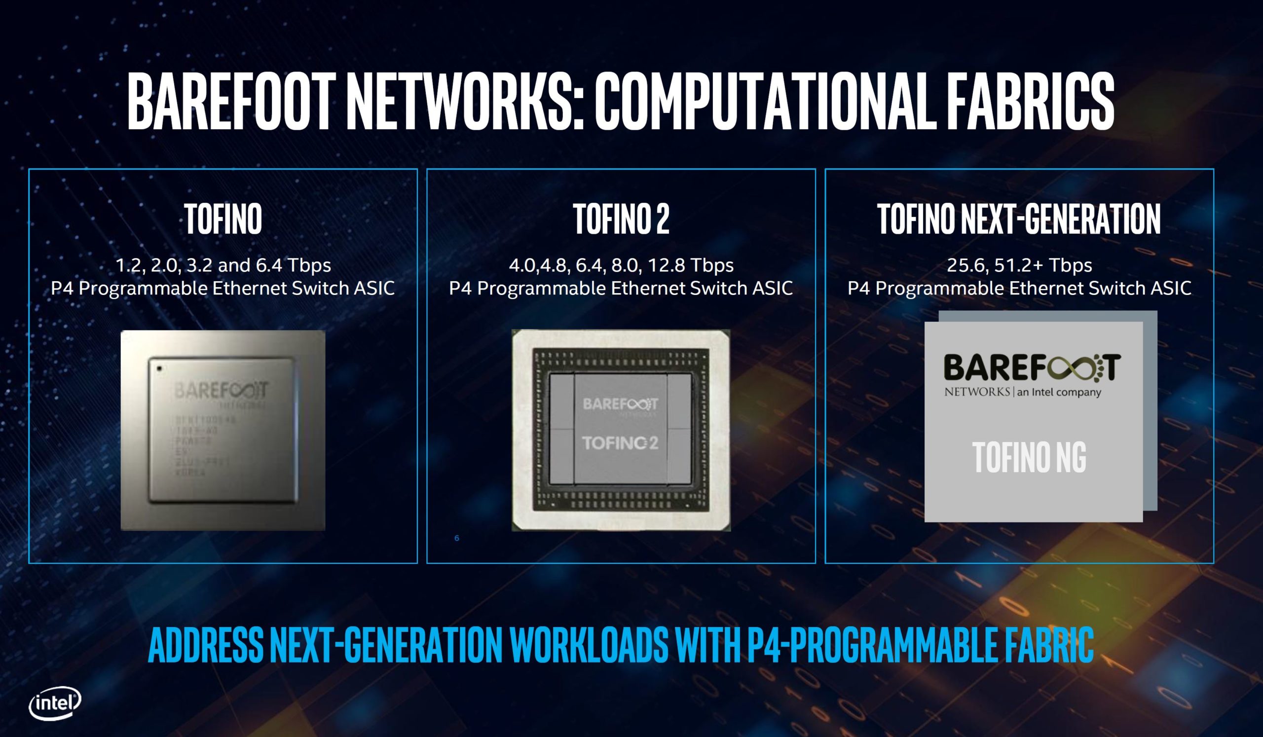 The only place I can find a mention of anything past Tofino 2 but I cannot find the original Intel slideshow that came from.
This is not Intel’s first foray into networking. The last time was when they bought Fulcrum and then nothing relevant came out of Fulcrum after that acquisition. They have also purchased Network Processor Unit (NPU) companies in the past. Not much ever comes out of Intel after these acquisitions.
I’m biased against Barefoot/Intel. Barefoot sees themselves as a premium brand and was trying to charge premium price because of their programmable pipeline, but I do not see the need for programmable pipeline, especially for openflow. Intel’s history with Fulcrum makes me suspicious of their future. That’s just opinion, not data, so take it for what it’s worth. I’m still salty over the Fulcrum’s disappearance after being purchased by Intel. For a while there was no real rival to Broadcom and that isn’t good for the industry.
- https://www.nextplatform.com/2018/12/04/programmable-networks-get-a-bigger-foot-in-the-datacenter-door/
- https://www.barefootnetworks.com/products/brief-tofino-2/
Broadcom
Broadcom is the giant in this industry, the king, the 800 pound gorilla. Broadcom was bought by Avago several years ago, and the whole company was renamed Broadcom.
Broadcom has two important families of chips in this space. One is the Strata XGS, the other is Strata DNX which was from a company Broadcom purchased called Dune. The XGS are the single ASIC type that we’ve been talking about in this article. The Dune chipset can be used for chassis devices or in fixed-form-factor if you need large tables. The Jericho 2 is the chip that can be used standalone or with a fabric chip, which is called the FE9600
Even in the XGS line there are several sub-species. The one the hyperscalers focus on is Tomahawk, which focused on speed. The Trident line has more features, I think they call this an edge services line. They have even more Ethernet chips with lower throughput, but we aren’t be concerned about them for this article. In general, Tomahawk is focused on hyperscalers, Trident is focused on Enterprise, and Jericho/Dune is focused on Services Providers.
Broadcom is like Intel in the CPU space. They go in waves in which they are the clear leader and there is almost no competition, then they seem to slow down and competition breaks out. We are at that point in the cycle right now with lots of competition, though Broadcom has stepped up their game in the latest Tomahawks to really put pressure on their competition. This is very good for the industry. Since Ian Cox is back at Broadcom they seem to have gotten themselves back in shape! :)


- https://www.youtube.com/watch?v=n9bUEb1v0pU Jericho 2
- https://www.nextplatform.com/2019/12/12/broadcom-launches-another-tomahawk-into-the-datacenter/
- https://www.broadcom.com/products/Ethernet-connectivity/switching/strataxgs
- https://www.broadcom.com/news/product-releases/broadcom-ships-jericho2
- https://www.broadcom.com/company/news/product-releases/52196
- https://www.nextplatform.com/2019/06/24/bringing-big-bandwidth-to-large-enterprises/
Cisco
If you hadn’t heard before, Cisco is selling merchant silicon chips to third parties. Not expected. They bought a company called Leaba, which was started by several of the founders of Dune. In general I would be wary of using Cisco as a provider, they’ve not done this before and it doesn’t fit their regular business model. However the Dune/Leaba team is really good which is why this is interesting to me. It will be especially interesting to see how Cisco supports an SDK to external customers.
The Q100 is more like the Strata DNX/Dune family than the Tomahawk. It’s also used in products at Cisco including the 8200
Cisco has many different inhouse ASICs that they don’t sell to third parties. And they have several switch lines that use other Merchant Silicon.
- https://www.datacenterknowledge.com/cisco/why-cisco-got-merchant-silicon-market
- https://www.cisco.com/c/en/us/solutions/service-provider/innovation/silicon-one.html
Innovium
Innovium is startup that has been competing toe-to-toe with Broadcom in the highest throughput ASICs in the last several years. Many of the main people from Innovium came from Broadcom. It is a very good team of people. It’s interesting that Innovium has design wins even though Broadcom has really upped their game in the last several of years.
Innovium has raised $350M. I don’t know enough about these to know why it has required so much money, nor why investors think they can gain that back, other than that they are winning designs, that just shows how little I understand. I can understand why they’d need ~$100M because it is very expensive to build chips, but as they’ve made progress and are selling I don’t know why they’d need further money.

- TeraLynx 8
- TeraLynx architecture
- https://www.nextplatform.com/2020/05/11/innovium-stays-on-broadcoms-heels-with-teralynx-8-switch-chips/
- https://www.zdnet.com/article/network-chip-contender-innovium-scores-170-million-to-challenge-broadcom-prepares-for-the-400-gig-onslaught/
- https://www.nextplatform.com/2019/09/30/innovium-boosts-switch-chip-performance-without-a-process-shrink/
- https://www.nextplatform.com/2018/06/20/a-deep-dive-into-ciscos-use-of-merchant-switch-chips/
Mellanox
Mellanox is known as the InfiniBand company, but they also sell Ethernet chips. Mellanox was purchased by Nvidia this year. They have been selling Ethernet ASICs for many years. Mellanox also bought Cumulus, probably so that they can ensure that they have a good OS for their chipset.
Mellanox has been around a long time selling Ethernet switches (and NICs), longer than anybody else here except Broadcom. As far as I know, they are no outside vendors like Cisco, Juniper, Arista, etc. that sell Mellanox based switches. As far as I know, you can only get them in white boxes. I don’t know why this is. It’s a mystery to me.
Mellanox seems to be supporting many different open source software efforts, such as SONIC, and SwitchDev, in a way that I don’t see any most of these vendors except Broadcom which is also investing in SONIC. And as mentioned above, they also bought Cumulus. I think this demonstrates how important software can be for these ASICs.
- https://www.nextplatform.com/2020/03/26/mellanox-doubles-up-Ethernet-bandwidth-with-spectrum-3/
- https://www.mellanox.com/files/doc-2020/pb-spectrum-3.pdf
- https://blog.mellanox.com/2018/10/sonic-open-Ethernet-dream-come-true/
- https://www.nextplatform.com/2020/05/12/is-microsofts-sonic-winning-the-war-of-the-noses/
- https://www.sdxcentral.com/articles/news/mellanox-challenges-imposter-open-source-vendors-with-sonic/2019/09/
Nephos
Nephos is a spinout of Chinese chip giant MediaTek, focusing on these switch ASICs. They were aggressive in their rollout of a 6.4T chip several years ago, being one of the first out with 6.4T, but haven’t kept up with the competition since then. They don’t seem to have a future, but I don’t know. We’ll have to see.
Other topics
There are a lot more topics that can be covered around these chips, but I’m not covering them here.
- SERDES / analog speeds
- Instrumentation – This chips have added a lot of very sophisticated monitoring on chip
- Pipelines and packet processing – what is the effect of multiple pipelines and what is the impact
- The effect of multiple memories on these chips and what that means for fairness
- optics
As networks get large, the cost of the network is driven by the cost of the optics. The real money saving is not when you get a faster chip, but when the chip supports higher throughput SERDES.
Other resources
I’ve included links to resources throughout the post. I’d recommend the http://www.nextplatform.com specifically, they have a wealth of information and are generally fantastic.
You should probably just watch this video from Ian Cox talking about Tomahawk 4.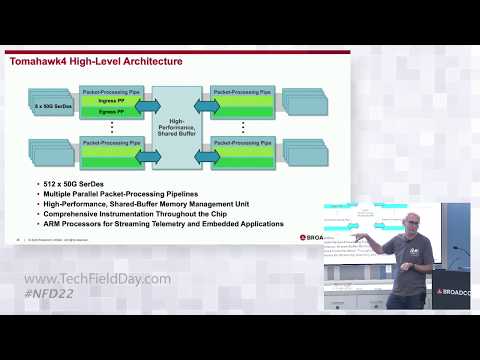 .
It’s based on Broadcom, where he works, but gives you a lot of the same information I have here, but in a different slant.
.
It’s based on Broadcom, where he works, but gives you a lot of the same information I have here, but in a different slant.
- https://www.nextplatform.com/2018/04/30/feeding-the-insatiable-bandwidth-beast/
- https://packetpushers.net/virtual-toolbox/list-merchant-silicon-manufacturers-chips/
- https://people.ucsc.edu/~warner/buffer.html
- https://www.nextplatform.com/2019/09/13/everyone-will-want-higher-bandwidth-and-more-ports-eventually/
- https://www.sdxcentral.com/articles/analysis/ocp-summit-moving-on-from-snow-white-and-the-seven-dwarfs/2019/04/
Comments
As an aside, this should be some kind of knowledge base or wiki, but I don’t know what that would be.
Let me know if I’m missing anything and/or I got something wrong. And updated sources would be fantastic.
Suzieq
Try out Suzieq, our open source, multivendor tool for network observability and understanding. Suzieq collects operational state in your network and lets you find, validate, and explore your network.